

Techniques Are Used in Assembling PCB Printed Circuit Boards
A jiggling component, a dangling coil or a finicky loose screw can affect the function of an electronic circuit board. This is why PCBs are subject to a variety of inspections throughout assembly. Specialized techniques can ensure that each component is firmly placed and soldered.
In the past, electronics components were connected using wires, but modern pcb printed circuit boards incorporate a number of key features to improve efficiency, accuracy and reliability. These include a multilayer substrate, etching to separate copper foil into individual conductors, pad areas for connecting component leads, vias to pass connections between layers of the board and a protective coating called solder mask.
Before a pcb printed circuit board is assembled, its components are checked for quality and consistency, and a bill of materials (BOM) is created to manage inventory. The BOM provides details about each component including its type, manufacturer, part number, quantity and more. This helps to reduce production costs and prevent mistakes during the assembly process.
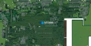
How Specialized Techniques Are Used in Assembling PCB Printed Circuit Boards
The bare board is populated with components using either surface-mount technology or through-hole technology (THT) to create a functional printed circuit board assembly (PCBA). A stencil is used to deposit solder paste on designated spots of the bare board, and then the assembler places the components onto the PCB, which are held in place by the solder. Once all the components have been soldered in, the bare board is inspected again to make sure all the connections are solid.
During the design phase, an ECAD system translates schematics into electronic drawings that show how each component is connected to one another. This allows engineers to test the functionality of their prototype and make adjustments before final production. Front-end engineering also involves selecting the laminate materials to use, and the PCB stack-up design identifies the need for plane layers, signal layers, dedicated routing channels, and specific material properties.
Once the design is complete, a layer of insulating material is placed over the copper. Then, chemical etching separates the copper into conductive tracks and pads for connections. The etching process also removes the insulating material, and a layer of solder mask is applied to protect the copper from oxidation, and to provide a smooth surface for reflow soldering.
Soldering: The reflow soldering process uses high temperatures to melt the metal alloy that connects the components to the PCB, ensuring strength and longevity. This method of assembly is more efficient than the THT technique and produces a cleaner, more reliable result.
In the reflow oven, the solder paste is heated up to the melting point of the components. This allows the solder to flow between the component and the copper, forming a strong bond. The reflow process can be automated using a pick-and-place machine, which uses mechanical or even vacuum-based movements to place each component on the board. This eliminates the need for intricate human touch and cuts down on assembly time. The reflow soldering process also uses an automated inspection system to detect errors, like shorts between traces, and faulty or improperly inserted connections.